はじめに
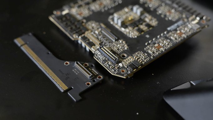
RTX 5090 の 裏面には、2つのコネクタがあります。それぞれのコネクタの用途を下記のように妄想していました。
赤が信号(PCIe)用、黄色が電源用ですかね。 https://t.co/jFBgTqU2nN pic.twitter.com/MFi1l3ywuB
— Vengineerの妄想 (@Vengineer) 2025年1月9日
- エッジに近い方が 電源用
- チップに近い方が PCIe用
では、実際は?
PCIe用コネクタ
下記のXの投稿、どうやら、エッジに近い方が PCIe用でした。
That daughterboard aka PCIe interface on the GeForce RTX 5090/5080 Founders Edition is something special. Foxconn uses a Black Core FR4 PCB featuring a layer of black thermoset resin sandwiched between two copper foil layers. pic.twitter.com/iVu2MFJg9g
— Andreas Schilling 🇺🇦 🇮🇱 (@aschilling) 2025年1月22日
画像が無くなると勿体ないので、引用します。
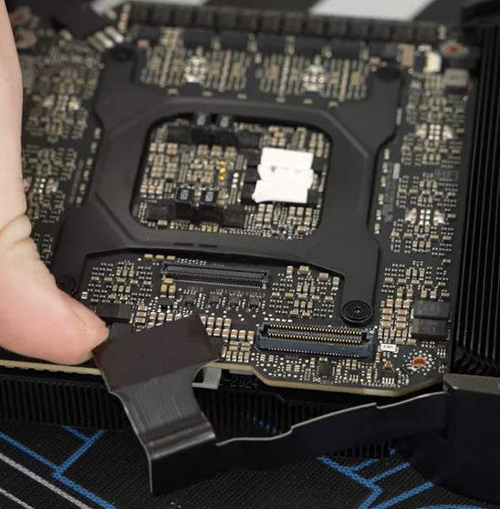
下記のビデオの12:35頃から、PCIe 部分のところが出てきます。
説明のために、PCIe 部分のキャプチャーを引用します。
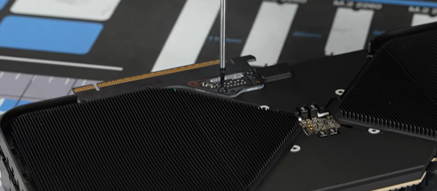
もう一つのコネクタ部分のキャプチャーを引用します。
また下記のビデオの 7:20 頃でも PCIe用コネクタという説明をしています。もう一つのコネクタは、I/O 用と言っています。
下記のXの投稿に、GB202の die shot に色づけしたものが載っています。
Interesting high lvl overview for #NVIDIABlackwell GB202:
— High Yield (@highyieldYT) 2025年1月28日
yellow = memory system (PHYs + controllers)
green = compute (excluding 3D/raster)
blue = level 2 cache
pink = I/O (PCIe 5.0 + 5x display)
unmarked areas = raster engines, NVDEC/ENC, command frontend, crossbar & MISC… pic.twitter.com/YNyT7H6Smz
I/O と PCIe の位置が一致しますね。
おわりに
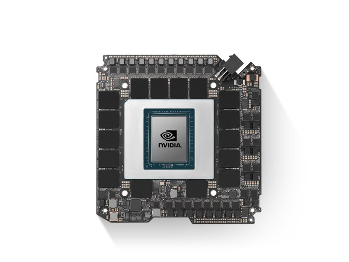
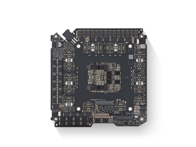
下記のXの投稿の写真がキレイです。
NVIDIA did release some high resolution images of the front and back of the compute PCB of the GeForce RTX 5090 Founders Edition. pic.twitter.com/mdsL5GKNBb
— Andreas Schilling 🇺🇦 🇮🇱 (@aschilling) 2025年1月23日
勿体ないので画像を引用し、記録に残します。